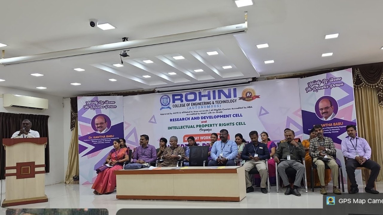

Value Added Course: VLSI Front-End Design for FPGA Implementation
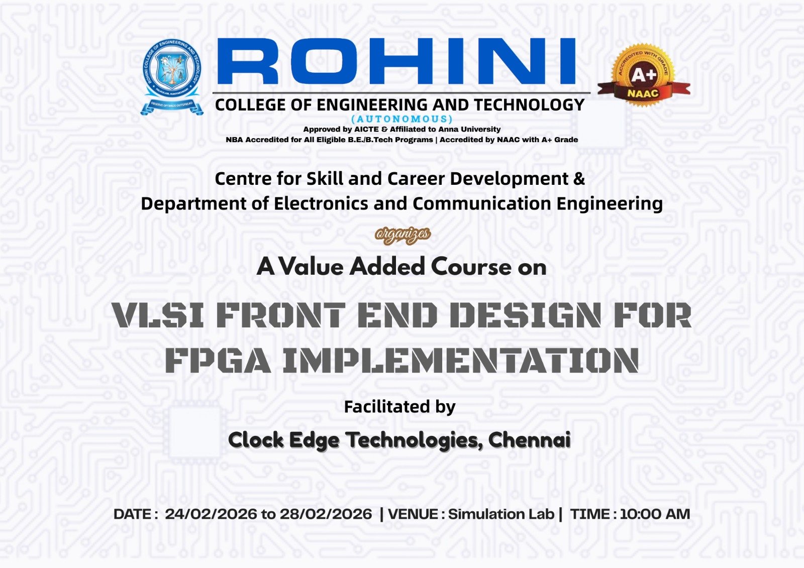
A Value Added Course on “VLSI Front-End Design for FPGA Implementation” was
conducted by Clock Edge Technologies Private Limited from 24 February 2026 to 28 February
2026. The course was designed to provide students with practical knowledge and hands-on experience
in digital design and FPGA-based implementation using Verilog HDL.
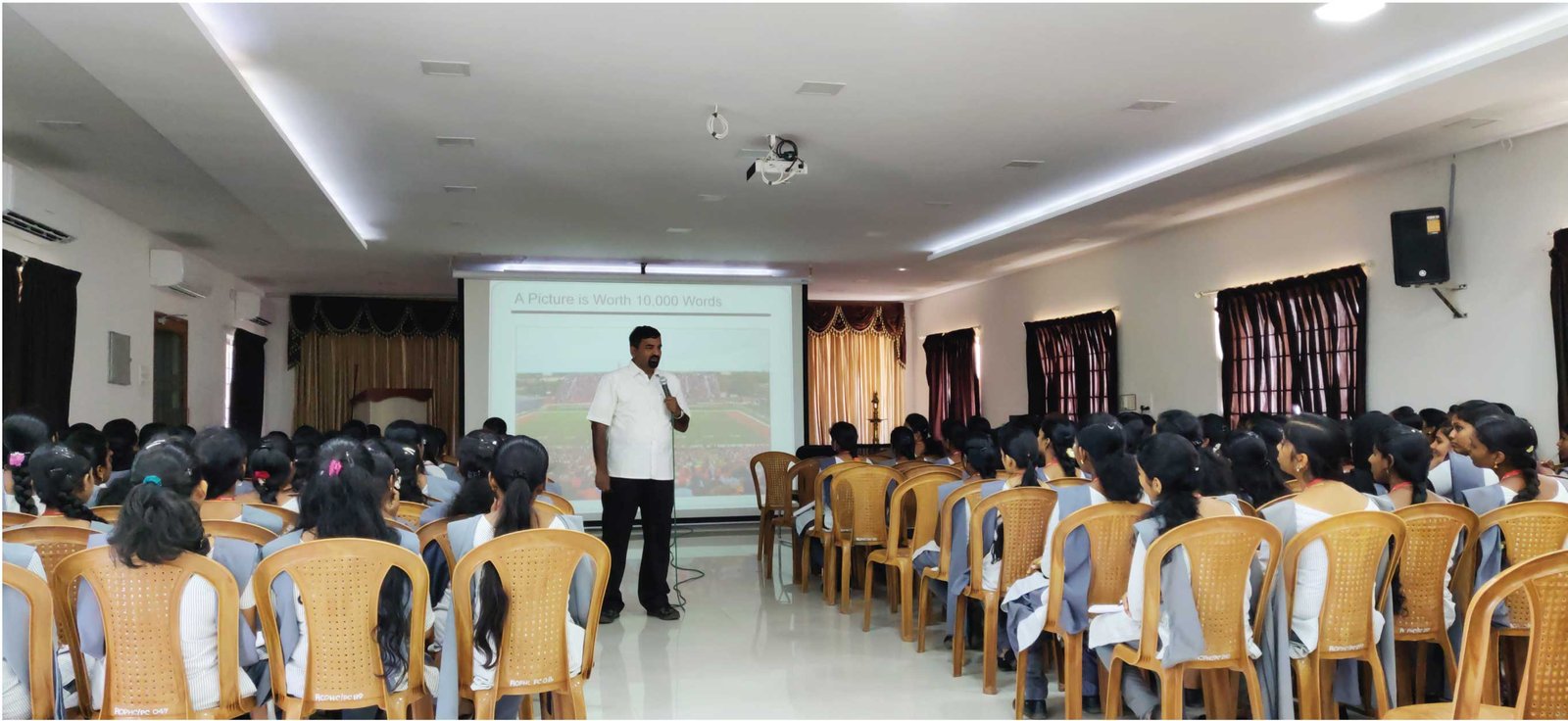
The training began with an introduction to the fundamentals of digital electronics, including number
systems, logic gates, combinational circuits, and sequential circuits. Students gained a clear
understanding of digital design concepts that form the foundation of VLSI front-end development.
A major focus of the course was on Verilog RTL (Register Transfer Level) coding. Participants
learned how to write synthesizable Verilog code for various digital circuits and understand the design
flow from coding to simulation and implementation. Hands-on sessions enabled students to develop
and test combinational and sequential logic circuits effectively.
Share This Article:
Share This Article: